


The short version
- OpenAI says its AI models improved AMD's next-generation flagship GPU design by up to 14% in PPA, the industry measure of power, performance and area, compared with "heavily optimized" designs.
- The models rewrote the chip's RTL, the code that describes its circuits. OpenAI says that delivered "roughly a year of progress" in under five months, and AMD has already put some changes into a design sent for manufacturing.
- AMD's next flagship CPU gained single-digit percentages. Neither chip is named, and it isn't clear whether the GPU is a gaming Radeon or a data-centre Instinct.
- Separately, startup Architect Labs claims its AI-designed Frostbite CPU is 4.6 times more efficient than a comparable core, but only in simulation.
What OpenAI announced
OpenAI published a research post, "Advancing chip design with our models", dated November 18; Tom's Hardware and others reported it on November 20. The key line: working with AMD, it has "seen up to 14% improvement relative to heavily optimized baselines" on AMD's "flagship GPU IP".
AMD has already used the results. According to OpenAI, it "already included some of these changes in a recent design it sent for manufacturing", and added others to its production design files. AMD also verified "single-digit percentage gains" across key blocks of its upcoming flagship CPU.
AMD CEO Lisa Su posted that she was "proud of these fantastic results", according to Stocktwits and AIM, which reported AMD's shares rising about 5% on the day.
What the 14% does and doesn't mean
The headline number needs care:
- "Up to" means the best case, not an average across the chip.
- PPA bundles three things. OpenAI didn't say whether the gain was in power use, speed, chip area or a mix.
- Which parts of the GPU were changed, and how much of the chip they make up, isn't disclosed.
- Which chips these are isn't stated. OpenAI only says "next generation flagship GPU and CPU". Calling it RDNA 5 or Zen 7 would be a guess.
- Which AI model did the AMD work isn't named either.
There's also a business link worth knowing. In October 2025, AMD agreed to supply OpenAI with 6 gigawatts of Instinct GPUs, starting with the MI450, and gave OpenAI a warrant for up to 160 million AMD shares that vests as the deal grows. Both companies benefit from good news about the partnership.

Image: AMD
How AI changed the design
A chip starts life as code. Engineers write its circuits in a hardware description language such as SystemVerilog, at what's called the register-transfer level, or RTL. Tools then turn that code into transistors and lay them out on silicon. Small changes to the RTL can make a block smaller, faster or less power-hungry, but finding them takes expert engineers months.
OpenAI says its models rewrote that RTL, and that Synopsys' tools checked the new code behaved exactly like the old and measured the PPA trade-offs. "We've observed the model reason about RTL at the level of an expert microarchitect," OpenAI wrote.
It has tried the same on its own chip. On Jalapeño, an AI inference chip OpenAI is building with Broadcom, model-suggested changes cut standard-cell area by about 13% in one unit and 10% in another, and OpenAI says those were "silicon proven". It's also training a model with Synopsys, called GPT-Synopsys, to use chip design software the way human experts do.
OpenAI is upfront about some limits in its own tests: some clock-speed figures were estimates rather than measured after full synthesis, and designs written from scratch left out features like performance counters, which may flatter their scores.

Image: Zerocade
AI in chip design isn't new, but this goes further
Chip companies have used machine learning in later design stages for years:
- Google's AlphaChip, published in 2021, places blocks on a chip's floorplan and has been used on every Google TPU since 2020, though its method has been disputed by some researchers.
- Cadence Cerebrus, launched in July 2021, tunes the steps that turn a design into a layout.
- Nvidia's ChipNeMo, shown in October 2023, is a language model that helps its chip engineers.
What's different here is that a general AI model is editing the design itself, and a major chipmaker says the results are going into products.
The AI-designed CPU
On the same day, Notebookcheck covered Frostbite from Architect Labs, a Palo Alto startup that raised $24 million in June. Its AI agents designed a new kind of CPU end to end: a compiler, a new instruction set, the RTL and the final layout.
| Frostbite | Claim |
|---|---|
| Design | A grid of small tiles that pass work between neighbours, with no central scheduler |
| Process | 7nm, 500MHz in the final layout |
| Efficiency | 4.59 times the performance per watt of an unnamed reference core, averaged across 25 workloads |
| Area | 8.77 times the performance per area |
| Status | Simulation only; no chip has been made |
The results vary hugely by task, from 23 times better on one workload to just 1.15 times on another. It hasn't been tested on standard benchmarks like SPEC or against modern high-end cores. Architect Labs plans to release the design and an FPGA test platform. On paper, it's an interesting research result, not something heading to a PC.
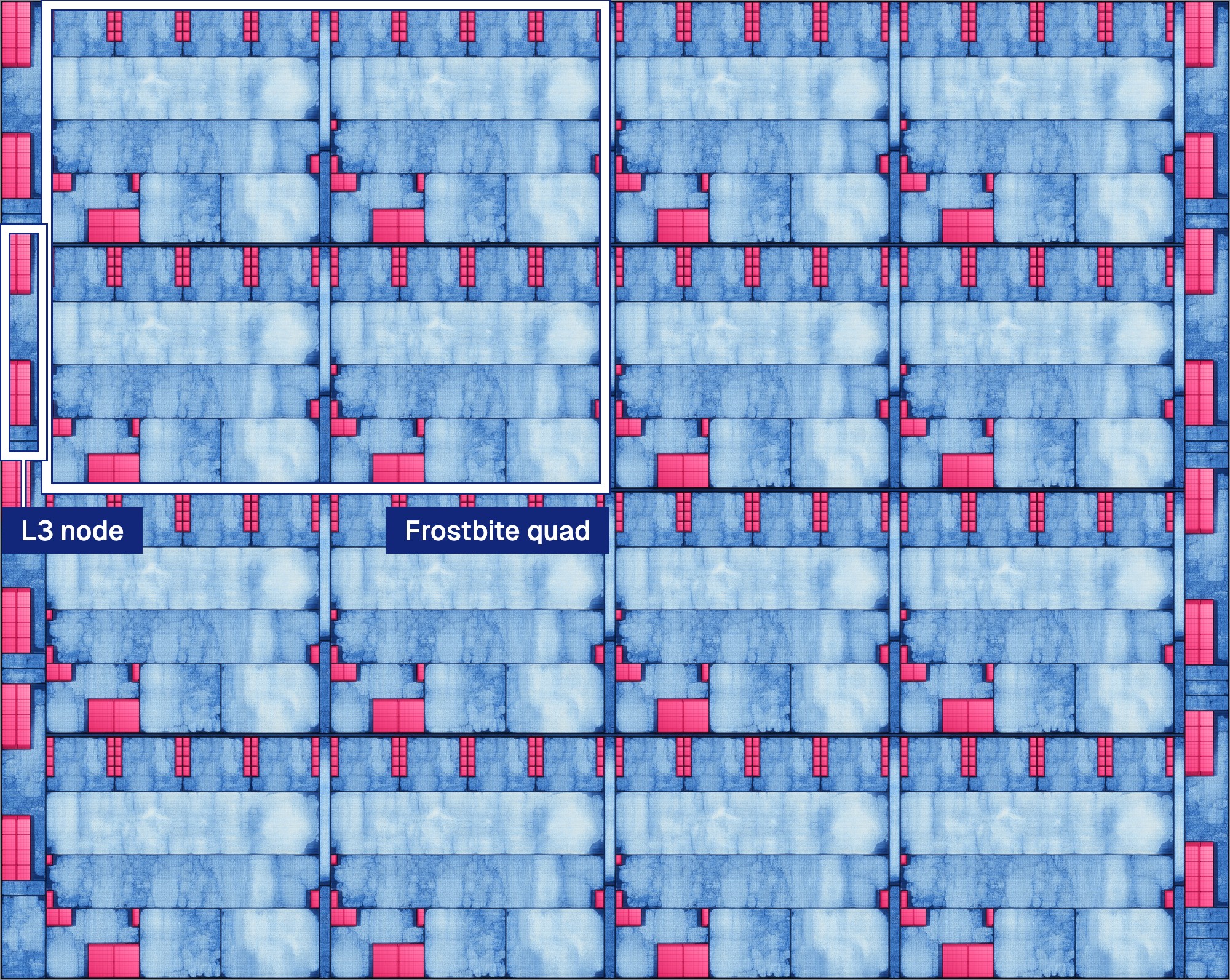
Image: Architect Labs
What it means for gamers in India
If the GPU in question is a future Radeon, AI-tuned blocks could mean slightly faster or more efficient cards. That's a big "if", and any gain would be one factor among many in the final price. For now, Radeon cards in India sit well above their launch prices: at PrimeABGB, an RX 9070 XT costs about ₹1,12,000-1,18,000 and an RX 9060 XT 16GB about ₹64,800-82,800.
There's a local link too. AMD's Bengaluru campus, opened in 2023 as its largest design centre worldwide, works on its CPUs and gaming and data-centre GPUs, and AMD said in 2023 that a quarter of its global workforce was in India.
What to watch
Watch for AMD to name the GPU and CPU involved, for independent detail on what the 14% covers, and for Architect Labs' FPGA release to show whether Frostbite's simulated gains hold up.