
The short version
- A hardware researcher who goes by Kate (kate-land on GitHub) has unlocked Nvidia's CMP 170HX mining card into an A100-class card with up to 80GB of memory.
- The method is voltage glitching: precisely timed dips in power at boot trick the chip into accepting new fuse settings that undo Nvidia's restrictions.
- In one FP16 benchmark the unlocked card scored about 18% higher than a retail A100. Nine of ten 8GB cards she modded reached a healthy 80GB.
- It's permanent, risky and slow, taking 1 to 48 hours per card. A real A100 80GB lists at about ₹10 lakh to ₹20 lakh in India.
What the CMP 170HX is
During the 2021 crypto boom, Nvidia launched CMP (Cryptocurrency Mining Processor) cards so miners would stop buying gaming GPUs. The CMP 170HX was the top one. It never appeared on Nvidia's official CMP page, but surfaced in September 2021 mining Ethereum at about 164 MH/s.
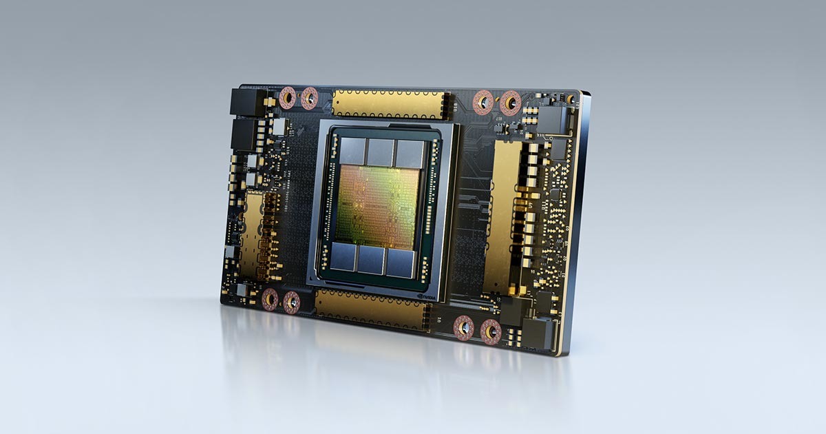
Inside is the same GA100 chip as Nvidia's A100 data-centre GPU, but heavily cut down:
- 70 of the chip's 128 SMs (streaming multiprocessors) switched on
- 8GB or 10GB of HBM2e memory
- PCIe locked to Gen 1 at x4, about 0.85GB/s
- FP32 maths deliberately throttled, no NVLink and no display outputs
When Ethereum moved off mining in September 2022, these cards flooded the used market for a few hundred dollars. In 2026 a software tool, cmpunlocker, managed to open up more of the memory and PCIe Gen 2, and prices jumped past $1,000.

Image: Nvidia
How the fuse glitch works
Kate published her write-up on November 10, with the board designs and code on GitHub. Tom's Hardware, Hardware Busters and others reported it on November 12.
Step 1: the fuses. Every GA100 has 16,384 eFuse bits, tiny one-time switches burned at the factory. They record which SMs, memory channels, NVLink links and PCIe speeds are disabled. Normally, burning a fuse can only restrict a chip further.
Step 2: the loophole. Part of that fuse area works as a log. Its entries replay at every boot, and a newer entry overrides an older one. So writing a fresh entry can clear a restriction without un-burning anything. On retail cards, a security bit blocks those new entries.
Step 3: the glitch. Kate removed a tiny resistor so the GPU no longer controls its own voltage regulator, then wired in a small STM32 microcontroller board that sends its own signal instead. It drops the core voltage for a split second just as the fuse controller starts up. In some of those glitched states, the security bit reads as off, and new fuse entries are accepted.
Step 4: repeat. A small single-board computer puts the PC to sleep and wakes it every few seconds for a fresh boot, over and over, until a glitch lands. That took between 1 and 48 hours per card. Before any of this, she disabled the chip's genuinely faulty units first, since fuse changes can't be undone.
It also shows that much of the gap between a cheap mining card and a $20,000 A100 was a business decision written into fuses, not broken silicon. Our chip binning guide explains how makers usually split one chip into many products.
What it unlocked
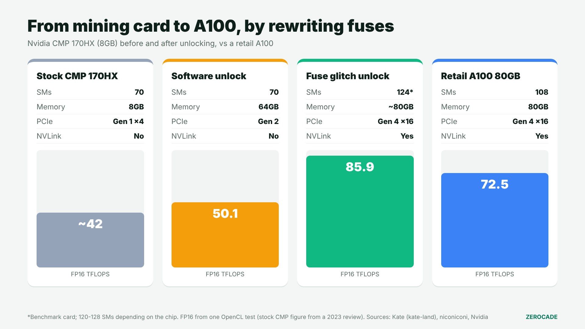
Image: Zerocade
| Stock CMP 170HX | Software unlock | Fuse glitch unlock | |
|---|---|---|---|
| SMs | 70 | 70 | 120-128, varies by chip |
| Memory (8GB card) | 8GB | 64GB | 64-80GB |
| PCIe | Gen 1 x4 | Gen 2 | Gen 4 x16 (with a capacitor mod) |
| NVLink | No | No | Yes (with a board mod) |
A retail A100 has 108 SMs, so a fully glitched card can actually have more active cores than the real thing. On her benchmark card, with 124 SMs and about 80GB:
- FP16: 85.9 TFLOPS, against 72.5 for a retail A100 and 50.1 for a software-unlocked CMP
- FP32: 22.8 TFLOPS, against about 0.39 TFLOPS for FMA maths on a stock CMP
- Memory bandwidth: about 1,883GB/s read, close to Nvidia's 1,935GB/s spec for the A100 80GB PCIe
AI tools like vLLM and SGLang ran across the full 80GB. ECC, MIG and the video decoders are now switched on but untested.
The catches
These are big:
- It's permanent. Fuses can't be un-burned, and some glitch states left cards unusable.
- It needs real soldering skill: removing tiny surface-mount parts and wiring to test points.
- Results vary by chip. The voltage waveform has to be tuned for each die. One of ten 8GB cards stopped at 64GB, and 80GB on the 10GB version is unproven.
- The numbers are limited. One OpenCL benchmark on one card, as PBX Science points out.
- NVLink needs extra board and software changes that Kate hasn't published.
- The cards are passive and need server-style airflow.
Kate says she reported the flaw to Nvidia's security team before going public, and published because another researcher had found it independently. Nvidia hasn't commented publicly. Since it's a hardware design issue, there's little it can do about cards already sold.
Prices, and why this matters
Used CMP 170HX listings on eBay now run from about $3,200 for the 8GB model, up from a few hundred dollars in 2023. An A100 80GB costs around $20,000 in the US. In India, RP Tech lists the PCIe card at ₹19,75,000 on enquiry, while cloud provider E2E Networks puts it at ₹10 lakh to ₹11.5 lakh. We found no Indian listings for the CMP 170HX.
For gamers, there's no direct benefit: these cards have no display outputs. But it's another sign of how desperate the AI crowd is for memory, the same pressure behind stripped RTX 5090s in China. An 80GB card for a fraction of an A100's price can run large language models that a 32GB RTX 5090 can't fit.
What to watch
Kate says her next target is a deeper glitch that could give debug-level access to the chip. Watch for an Nvidia statement, and for used CMP 170HX prices, which on paper are likely to keep climbing.