

The short version
- Yield is the share of chips on a silicon wafer that come out working. The rest are thrown away or sold as cut-down models.
- Intel CEO Lip-Bu Tan said on November 19 that its 18A process yield "was horrible" when he took over, and is now at 70%. He didn't say exactly how Intel measures it.
- Big chips suffer most: on paper, a die six times larger can cost about 11 times more per working chip.
- 18A makes the CPU tiles in Intel's Core Ultra Series 3 (Panther Lake) laptops, which start at ₹1,27,990 in Samsung's Galaxy Book6 range in India.
What Intel said
Tan made the comment at the TomorrowX conference, reported by Tom's Hardware: "When I took over, 18A yield was horrible; now we are at 70%." He became CEO in March 2025.
One caveat matters. Tan didn't say which kind of yield he meant. Chipmakers track several: how many dies work at all, how many hit their target speeds and power, and how many end up as sellable products. These can be very different numbers, which is why earlier reports about 18A disagreed so much.
The same week, Microsoft became the first company to publicly commit to Intel's EMIB packaging for its own chips, as we covered in Intel's 18A-P customer news.
Step 1: chips start as a wafer
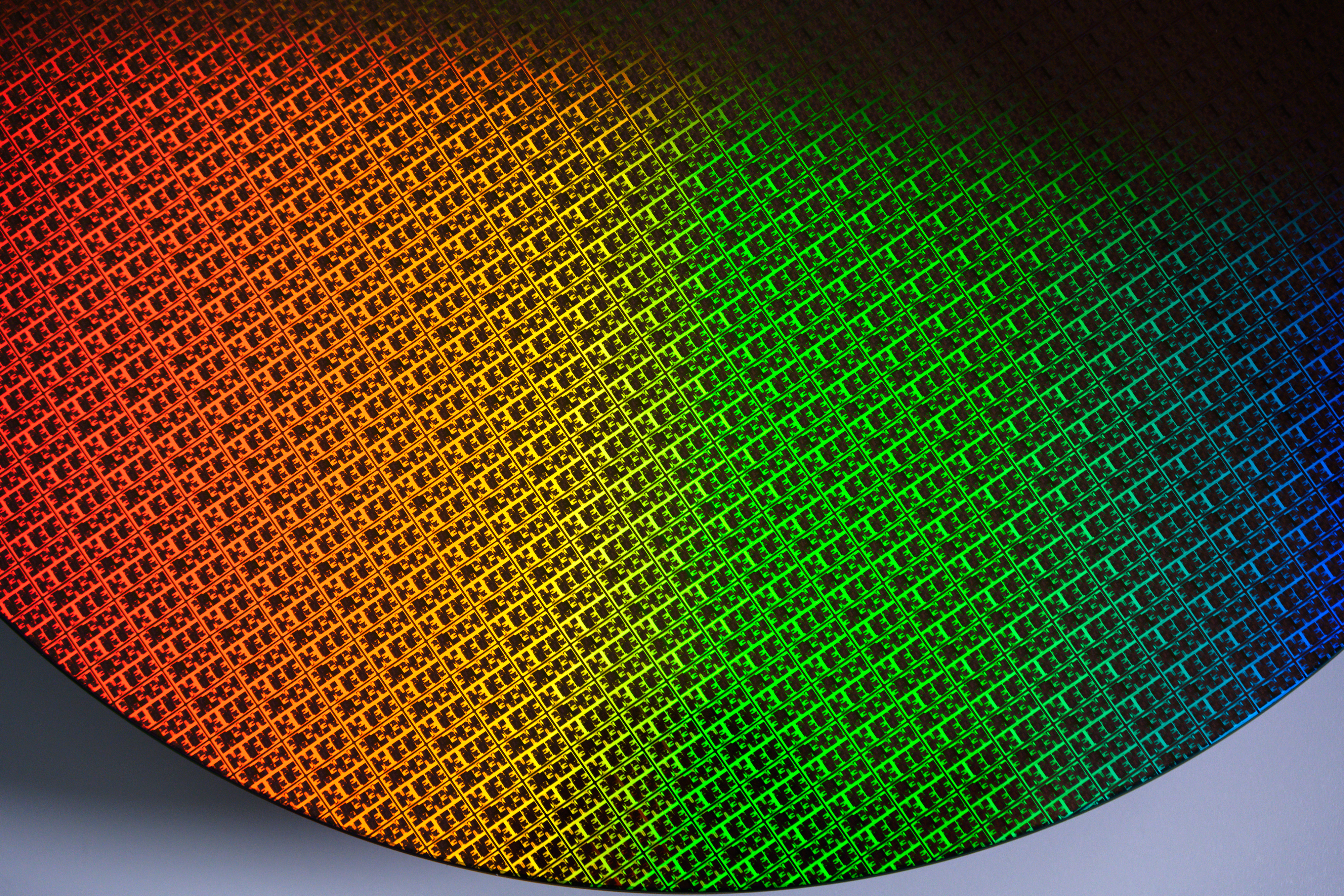
Processors are made on round silicon wafers 300mm across, with an area of about 70,700 square millimetres. Hundreds of identical chips, called dies, are printed across each one in a grid, then the wafer is cut up.
How many dies fit depends on their size. A simple formula estimates it, accounting for the partial dies lost at the round edge:
- A 70.6mm² die, the size of one AMD Zen 5 CPU chiplet, fits about 922 times.
- A 750mm² die, the size of the GB202 chip in the RTX 5090, fits only about 70 times.

Image: Micron
Step 2: defects land at random
No factory is perfectly clean. Specks of dust, tiny flaws in the silicon and printing errors land in random places on each wafer. Engineers measure this as defect density, written D0, in defects per square centimetre.
If a defect lands on a die, that die usually fails. So the chance a die survives depends on two things: how dirty the process is, and how much area the die covers. The classic estimate is the Poisson model, where yield equals e to the power of minus (die area times defect density).
You don't need the maths to get the point. A tiny die is like a small target in a hailstorm: most of them dodge every hailstone. A huge die is a big target, and many get hit.
Step 3: why big chips cost so much more
Here's a worked example of our own, using a defect density of 0.1 per square centimetre:
| Die size | Example | Dies per wafer | Yield | Working dies | Cost each on a $30,000 wafer |
|---|---|---|---|---|---|
| 70.6mm² | Zen 5 chiplet | ~922 | ~93% | ~859 | ~$35 |
| 100mm² | Small chip | ~640 | ~90% | ~580 | ~$52 |
| 600mm² | Large GPU | ~91 | ~55% | ~51 | ~$586 |
| 750mm² | RTX 5090's GB202 | ~70 | ~47% | ~35 | ~$867 |
The 600mm² die is six times the size of the 100mm² one but costs about 11 times as much per working chip. It loses twice over: fewer candidates per wafer, and a much higher chance each one is hit. That's part of why flagship graphics cards cost what they do. The $30,000 figure is the reported price of a TSMC 2nm wafer; TSMC doesn't publish prices, and its 3nm wafers have been reported at around $18,500-20,000.
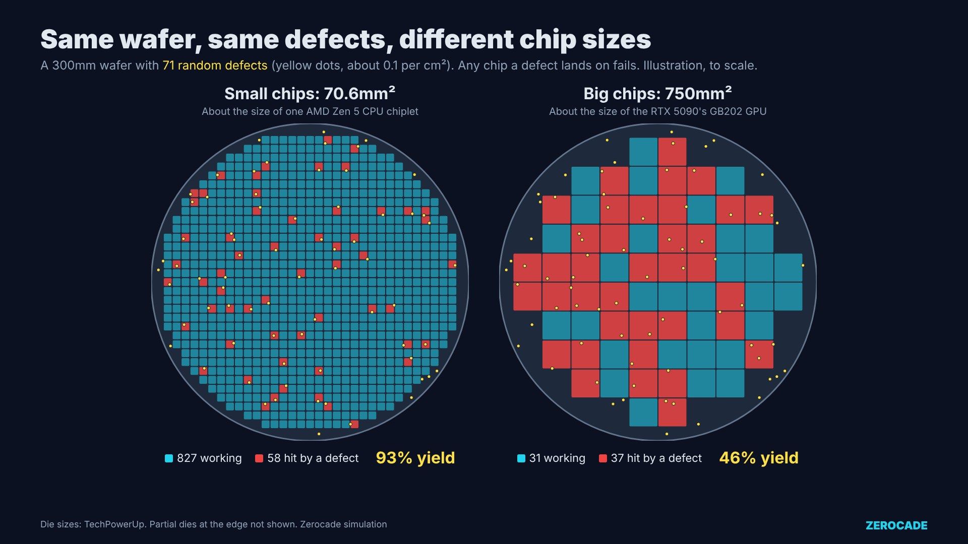
Image: Zerocade
Step 4: how chipmakers fight back
Chiplets. Instead of one giant die, AMD builds Ryzen processors from small CPU chiplets plus a separate I/O die. A defect only kills one small piece. Our chiplets guide covers how Intel and AMD each do it. Intel's Panther Lake is also tiled: its CPU tile is on 18A, but its graphics tile is made by TSMC.
Binning. A die with one broken core or shader cluster isn't always scrap. It can be sold as a lower model with that part switched off, which is how one chip becomes several products. See our chip binning guide.
Time. Yield improves as a factory learns where its defects come from. New processes usually start low and climb for a year or more.
Step 5: 18A's bumpy road
Intel's numbers have been hard to pin down, because different reports measured different things:
- August 2025: Reuters, citing unnamed sources, said only about 10% of 18A chips met spec that summer. Intel's CFO said the figure was too low but didn't give one.
- July 2025: analysts at KeyBanc estimated 55%.
- October 2025: Intel said yields were "not where we need them to be" and expected industry-standard levels in 2027.
- April 2026: KeyBanc's checks put it at about 65%.
- November 2026: Tan says 70%.
Intel has been here before. Its 10nm process, first promised for 2015, slipped to 2019 for volume production because yields improved more slowly than planned. Samsung's 3nm process also reportedly struggled, and reports linked that to the Galaxy S25 using Snapdragon chips instead of Exynos. Samsung never confirmed those figures.
Image: Intel
What 70% means for you
Using the same maths, moving a 100mm² die from 55% to 70% yield cuts the cost of each working chip by about a fifth. On paper, that helps Intel make Panther Lake chips more cheaply and in bigger numbers, and makes 18A more attractive to outside customers. It's also earlier than the 2027 target Intel gave a year ago, if Tan means the same kind of yield.
Don't expect cheaper laptops straight away, though. Only the CPU tile is on 18A, and memory prices are pushing laptop prices up. In India, Samsung's Galaxy Book6 laptops with Core Ultra Series 3 chips cost ₹1,27,990 for the 14-inch model, ₹1,78,990 for the Book6 Pro 14 and ₹2,42,990 for the Book6 Ultra. For the basics of what "18A" or "2nm" means, see our process node guide.
What to watch
Watch Intel's next earnings in January for an official yield update, and for Nova Lake desktop chips on 18A-P, which will show whether the gains carry over to Intel's next process.